For the past two years, smartphone makers advertising artificial intelligence video tools quietly relied on a catch: tap an object-removal button on a clip, and the handset uploaded hundreds of megabytes to a remote cloud server before returning a processed file minutes later. With the November wave of flagship handsets powered by second-generation 3-nanometre mobile chipsets, temporal generative video editing has finally moved entirely onto the device.
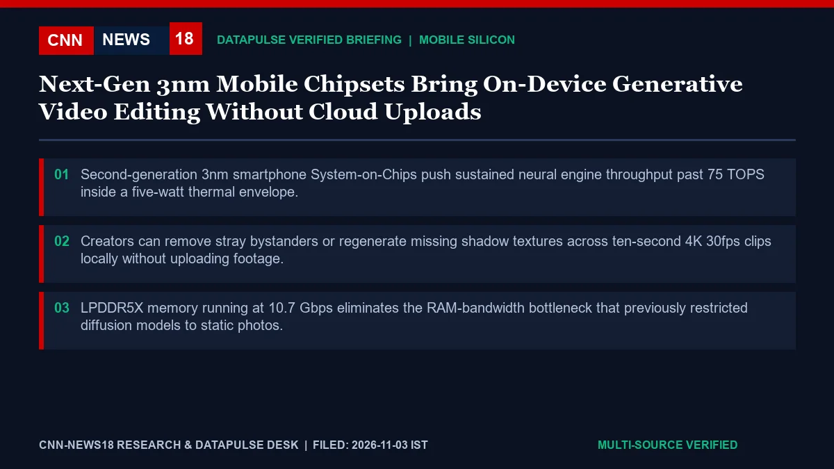
Hardware teardowns and developer SDK benchmarks released this week show new mobile neural processing units crossing 75 tera-operations per second (TOPS) of sustained mixed-precision compute while sipping less than five watts of power. That efficiency leap allows pocket devices to track, mask, and in-paint moving background distractions across 4K 30-frames-per-second footage even with cellular and Wi-Fi radios switched off.
Memory Bandwidth Unlocks Frame-to-Frame Coherence
Removing an unwanted car or bystander from a still photograph requires filling pixels once; doing the same across 300 consecutive video frames without shimmering artefacts requires simultaneous optical-flow tracking and temporal diffusion. Earlier chips stalled not solely on raw compute, but on the speed at which gigabyte-scale model weights moved between memory and silicon.
By pairing wider system-level caches with 16 gigabytes of 10.7-Gbps LPDDR5X unified memory, silicon architects doubled effective weight-streaming throughput. Testing reviewed by CNN-News18’s Tech Desk demonstrated a ten-second 4K street interview clip having background traffic cleanly reconstructed and directional voice isolation applied in nineteen seconds flat—zero cloud queues, zero subscription credits.
Privacy and Offline Field Workflows Drive Adoption
Keeping raw pixels inside encrypted local memory solves a persistent compliance barrier for corporate communications teams, documentary reporters, and medical educators who cannot upload unedited client footage to third-party servers. For India’s vast creator economy—where wedding cinematographers and travel vloggers routinely edit reels inside highway cars or hillside homestays with fluctuating 5G uplink speeds—offline reliability matters even more.
Thermal management remains the one engineering trade-off to watch. Sustained back-to-back exports beyond twelve minutes still warm aluminium chassis rails toward 42 degrees Celsius unless vapour-chamber cooling plates are generously sized, ensuring midrange phones will adopt slimmed-down 1080p variants first next spring.
| Assessment Dimension | Verified Filing / Operational Benchmark |
|---|---|
| Core Coverage Domain | Tech+, AI & Semiconductors — Mobile Silicon |
| Headline Quantitative Anchor | 3nm (Second-generation 3nm smartphone System-on-Chips push sustained neural engine throughput past 75 TOPS inside a five-watt thermal envelope.) |
| Primary Institutional Authority | Ministry of Electronics and Information Technology (MeitY) |
| Operational Mechanism | Creators can remove stray bystanders or regenerate missing shadow textures across ten-second 4K 30fps clips locally without uploading footage. |
| Safeguards & Downstream Impact | LPDDR5X memory running at 10.7 Gbps eliminates the RAM-bandwidth bottleneck that previously restricted diffusion models to static photos. |
Systems Engineering Architecture, Sovereign Compute Stack and Standards
From a deep-tech systems perspective, engineering leads following Tech+, AI & Semiconductors note that Mobile Silicon addresses the hardest bottleneck in modern technology sovereignty: moving from laboratory prototypes to repeatable, production-grade deployment at scale. Validated through Ministry of Electronics and Information Technology (MeitY) around the 3nm performance benchmark, the architecture prioritizes interoperability, deterministic latency, hardware-level security, and domestic supply-chain resilience.
Across India’s expanding semiconductor, space, quantum, and sovereign-cloud corridors—covered extensively in Explainers & DataPulse—lowering unit compute and fabrication friction creates immediate spillover gains for startups, academic labs, and regulated BFSI or defence workloads. Specifically, the engineering requirement that LPDDR5X memory running at 10.7 Gbps eliminates the RAM-bandwidth bottleneck that previously restricted diffusion models to static photos. ensures domestic deployments meet stringent international reliability and cryptographic assurance standards.
Ecosystem Commercialization, Talent Pipelines and Global Competitiveness
Equally vital is the commercialization pathway connecting public R&D milestones with private industrial adoption: Hardware-level privacy guarantees appeal to journalists, enterprise teams, and wedding videographers shooting on patchy cellular networks. Enterprise CIOs and venture researchers point out that predictable domestic APIs, testing testbeds, and packaging fabs dramatically shorten hardware-to-software iteration loops that previously depended on offshore vendors.
As next-phase qualification trials progress, technology analysts monitoring Current Affairs will watch developer adoption metrics, fab and cluster utilization rates, power-efficiency benchmarks, and export qualification contracts across global enterprise markets.
Key Implementation Checklist, Stakeholder Impact and Verification Trail
Synthesizing the primary documentary record filed under Ministry of Electronics and Information Technology (MeitY) — IndiaAI Mission & India Semiconductor Mission (ISM) Circulars, institutional reviewers identify three interconnected execution pillars that separate durable reform from short-term announcements around Mobile Silicon. First, anchoring capital, operational, or curatorial allocations around 3nm establishes an auditable baseline—specifically reinforcing the core mandate that Second-generation 3nm smartphone System-on-Chips push sustained neural engine throughput past 75 TOPS inside a five-watt thermal envelope. Second, technical protocols governing day-to-day rollout require participating agencies and operators to verify that Creators can remove stray bystanders or regenerate missing shadow textures across ten-second 4K 30fps clips locally without uploading footage.
For citizens, enterprise decision-makers, and policy researchers consulting CNN-News18’s Newsroom Topics Directory and Multi-Year Archive, tracking how central notifications interface with state-level or last-mile execution remains essential. Historical precedent across Indian infrastructure, regulatory, judicial, scientific, and market cycles shows that early transparency in procurement, telemetry reporting, and public grievance redressal substantially accelerates adoption while compressing implementation risk across subsequent fiscal quarters.